 Home
-
Hot News
-
Multiple Semiconductor Manufacturers Respond Urgently to the Impact of Japan's Sudden Earthquake
Author:netwing Time:2024-01-03 Browse:
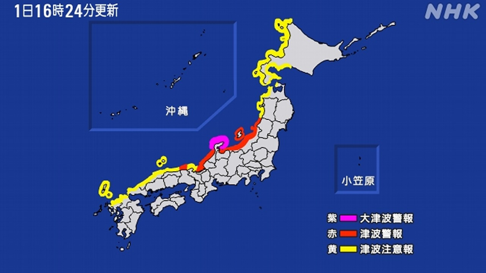
On the 1st, a strong earthquake with a magnitude of 7.6 occurred on the Neden Peninsula in Ishikawa Prefecture, Japan. This earthquake is the third largest in Japan since 2010, only following the 2011 Northeast earthquake and the 2015 Ogasawara Islands earthquake. Compared with the 311 earthquake, due to its smaller scale, poor concentration of industries in the area, and no radiation concerns, it is estimated that it will not cause supply interruption or order switching, and its impact on semiconductor industry is limited.
On January 2nd, according to the Japan Broadcasting Association (NHK), the Ishikawa Prefectural Police Headquarters stated that as of 5:00 pm local time on January 2nd, the earthquake had caused 6 deaths.

One of the characteristics of Ishikawa Prefecture's economy is that more than half of the manufacturing industry practitioners work in the machinery related industry, and the per capita production of machinery manufacturing is also the highest in Japan.
The world's largest MLCC Japanese merchant Murata Manufacturing Company has multiple factories located in the earthquake area, namely SAW Filter and Komatsu Murata Manufacturing Company (WiFi, Bluetooth modules). Due to the global market share of Murata SAW Filter approaching 50%, its factory situation has also attracted industry attention. In response, the company's PR stated, "Due to the factory being closed during the New Year holiday, it has not been operational. While ensuring the safety of employees, we are currently confirming the damage to the facilities."
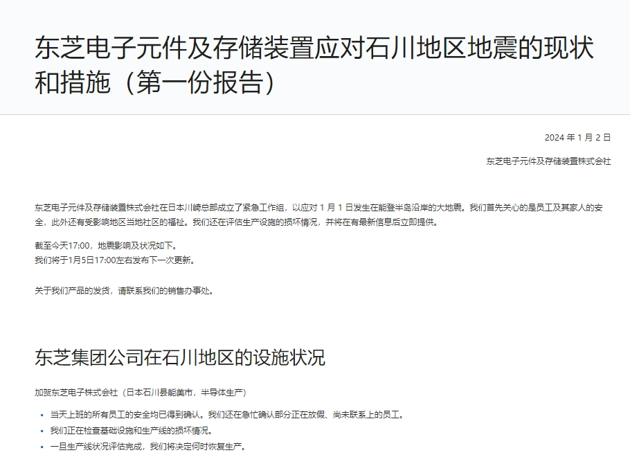
Toshiba also owns a power semiconductor factory in Ishikawa Prefecture, with a newly built 300mm (12 inch) wafer factory expected to enter mass production in 2024. Whether this will affect the production process or existing capacity remains to be monitored in the future. However, due to the fact that all newly built factories in Japan will adopt seismic resistant structures and have experience in dealing with them, it is estimated that the impact can be prevented and controlled.
On January 2nd, Toshiba officially issued a notice stating that the safety of all employees working that day had been confirmed, and some employees who were on vacation and had not yet been contacted were still being confirmed. The damage caused by the earthquake is still being evaluated.

The wafer foundry TPSCo, a joint venture between New Tang and Takata, is located near the epicenter of Ishikawa Prefecture, mainly supplying local Japanese customers. Takata and New Tang each hold 51% and 49% of the shares, with Takata leading the operation. The company has two 8-inch factories and one 12 factory located in Toyama Prefecture and Niigata Prefecture, near the epicenter of the earthquake in Ishikawa Prefecture. New Tang Company has not yet reported on the operational impact of TPSCo, and the actual impact remains to be observed.
TPSCo has been continuously planning to merge production capacity in Japan for a period of time, reducing equipment in uneconomical 8-inch factories and expanding to mainly 12 inch factories, mainly for special process and battery management IC production capacity expansion, supplying local customers in Japan.
As for the TSMC and UMC factories, as they are currently located in Kumamoto Prefecture, Kyushu and Mie Prefecture, Honshu respectively, and are not affected by the disaster, TSMC Kumamoto Plant 1 still maintains its production plan for 2024, and it is estimated that there will be no significant impact on the Japanese operations of the two companies.
Japanese semiconductor equipment manufacturer KOKUSAI ELECTRIC has a production base in Toyama Prefecture, and the company said, "So far, there have been no reports of damage to our base. We are currently confirming internally and have not yet obtained any information from the site (such as major chaos)."
*The content of the article is reproduced from the official account of ChipVision. If there is infringement, please contact to delete
Previous Article:Suspected of fraudulent issuance of amethyst storage and taken mandatory measures
Next Article:News: The first functional semiconductor made of graphene is born
 Contact Us:86-755 0755-84501787
 Mailbox:jessie@szlitus.com
 Headquarters Address:1808, Building A, Rongde International, Henggang Street, Longgang District, Shenzhen


Skype
Copyright © 2005-2023Shenzhen Lites Electronic Technology Co., Ltd All Rights Reserved Record number: Guangdong ICP backup2024178703-1 Background login